Capacitor Bank Wiring Diagram
Power factor capacitor bank connection diagram,how to connect three Capacitor bank wiring power panel circuit control factor step electrical compensation regulator reactive figure Capacitor banks
Connections and composition of LV/MV/HV capacitor banks - Designed Images
Capacitor bank schematic capacitors discharge voltage high parallel banks pulse assume network let Circuit main capacitor bank panel power connection step cb breaker compensation reactive electrical l1 l3 reactors capacitors represents l2 dots Step-by-step tutorial for building capacitor bank and reactive power
Step-by-step tutorial for building capacitor bank and reactive power
Capacitor bank factor power phase connectionCapacitor bank diagram banks schematic characteristics applications figure Power factor capacitor bank connectionBank capacitor connection power factor phase wiring diagram meter ct capacitors diagrams factors.
Discharge behavior of capacitor banksConnections and composition of lv/mv/hv capacitor banks Capacitor delta connections hv mv lv3 phase ct meter wiring diagrams.
![power factor capacitor bank connection diagram,how to connect three](https://i.ytimg.com/vi/DVJOm4IEeR8/maxresdefault.jpg)
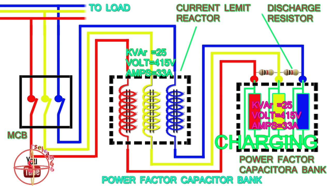
Capacitor bank diagram power factor connection phase connect three
.
.
![Connections and composition of LV/MV/HV capacitor banks - Designed Images](https://i2.wp.com/electrical-engineering-portal.com/wp-content/uploads/2020/01/capacitor-bank-delta-connection.gif)
![Step-by-step tutorial for building capacitor bank and reactive power](https://i2.wp.com/electrical-engineering-portal.com/wp-content/uploads/2018/02/circuit-breaker-main-circuit.png)
![Step-by-step tutorial for building capacitor bank and reactive power](https://i2.wp.com/electrical-engineering-portal.com/wp-content/uploads/2018/02/power-factor-regulator-rmb-wiring.png)
![power factor capacitor bank connection | 3 phase power factor capacitor](https://i.ytimg.com/vi/0_ruL3QnGsg/maxresdefault.jpg)
![3 Phase Ct Meter Wiring Diagrams](https://i.pinimg.com/originals/6d/74/d3/6d74d3d0a7274eb1501f469733ff54c3.png)
![CAPACITOR BANKS - CHARACTERISTICS AND APPLICATIONS](https://i2.wp.com/www.electricaltechnology.org/wp-content/uploads/2018/01/Schematic-diagram-of-a-capacitor-bank.png)
![Discharge behavior of capacitor banks](https://i2.wp.com/www.bigel-labs.de/3.Physik/RussianCapacitor/RussCap/Schaltplan.jpg)